In semiconductor manufacturing, a single microscopic particle clinging to a silicon wafer surface can turn a high-value chip into scrap. As device geometries continue to shrink toward single-digit nanometer nodes, the tolerance for contamination has become vanishingly small. Particles measuring just a fraction of a micron—invisible to the naked eye—can create open circuits, short circuits, or reliability failures in finished devices.
This is why wafer cleaning has evolved from a simple preparatory step into one of the most critical processes in semiconductor fabrication. Among the various cleaning technologies available today, ultrasonic cleaning stands out as the preferred choice for silicon wafer processing. But what makes ultrasonic cleaning uniquely suited to the exacting demands of wafer manufacturing?
The answer lies in three fundamental advantages: its ability to reach every microscopic crevice on the wafer surface, its non-contact nature that eliminates mechanical damage to delicate silicon substrates, and its capacity to deliver consistent, repeatable results batch after batch. This article explores why ultrasonic cleaning has become the gold standard for silicon wafer processing and how Whale Cleen ultrasonic cleaning machines can help semiconductor manufacturers achieve the highest levels of cleanliness and yield.
Before understanding why ultrasonic cleaning is preferred, it helps to understand what makes wafer cleaning uniquely challenging.
Silicon wafers are subjected to dozens of cleaning cycles throughout the fabrication process—before oxidation, after etching, before deposition, after CMP (chemical mechanical planarization), and at numerous other stages [5†L17-L19]. At each stage, the wafer surface carries different types of contaminants that must be completely removed before the next process step.
The main categories of wafer contaminants include:
Particle contamination: Microscopic dust, silicon debris from sawing and grinding, abrasive particles from CMP slurries, and metal fragments from handling equipment. Even particles smaller than 0.1 microns can cause fatal defects in advanced nodes [1†L33-L36].
Organic residues: Photoresist residues after patterning, oils and greases from handling equipment, and organic solvents that leave molecular films on the wafer surface [1†L14].
Metallic contaminants: Trace metal ions from process chemicals, equipment wear particles, and airborne metal dust that can migrate into device structures during high-temperature processing, creating recombination centers that degrade electrical performance.
Native oxide and chemical residues: Thin oxide layers that form naturally on silicon surfaces, plus residues from acid or alkaline cleaning solutions that must be completely rinsed away [1†L43-L45].
Traditional cleaning methods—manual brushing, high-pressure spraying, and chemical immersion alone—struggle to address these contaminants comprehensively. Mechanical methods risk scratching delicate wafer surfaces [3†L22]. Chemical methods alone cannot remove physically adhered particles [1†L7-L8]. And neither approach can reliably penetrate the microscopic trenches, via holes, and fine patterns that characterize advanced semiconductor devices [6†L30-L31].
This is where ultrasonic cleaning technology offers a fundamentally superior solution.
Ultrasonic cleaning relies on a physical phenomenon called cavitation. High-frequency sound waves—typically in the 20 kHz to 100 kHz range—are transmitted through a cleaning liquid, generating millions of microscopic vacuum bubbles that rapidly grow and implode. When these bubbles collapse, they release localized high temperatures and shock waves that blast contaminants away from the wafer surface [7†L8-L14].
Advantage 1: Reaches Every Microscopic Crevice
Unlike high-pressure spraying, which relies on linear fluid flow that cannot turn corners or penetrate tight spaces, ultrasonic cavitation occurs throughout the entire liquid medium wherever sound waves can travel. This means that every surface the liquid contacts—no matter how complex the geometry—receives the same cleaning action. For silicon wafers with deep trenches, high-aspect-ratio vias, and fine line patterns, ultrasonic cleaning reaches areas that mechanical methods simply cannot access [1†L18-L20].
Advantage 2: Non-Contact, Damage-Free Cleaning
Silicon wafers are brittle and easily damaged. Traditional scrubbing methods create mechanical contact that can leave microscopic scratches—scratches that become defect nucleation sites in subsequent processing [3†L22]. Ultrasonic cleaning is inherently non-contact, using only the energy of collapsing cavitation bubbles to remove contaminants. The wafer never touches any solid cleaning implement, eliminating the risk of mechanical damage [3†L21-L22]. For delicate structures like low-k dielectric layers and fine copper interconnects, this non-contact attribute is essential for maintaining device integrity.
Advantage 3: Reduces Chemical Dependency and Process Complexity
A frequent misconception is that ultrasonic cleaning relies on aggressive chemicals. In fact, the mechanical energy of cavitation does most of the contaminant removal work, allowing milder cleaning solutions to achieve the same or better results. Studies have shown that ultrasonic technology achieves excellent removal of organic contaminants and particles without requiring the high chemical concentrations used in traditional wet benches [1†L33-L36]. This not only lowers operating costs but also reduces hazardous waste generation and simplifies chemical handling requirements.
Advantage 4: Consistent, Repeatable Results
Manual cleaning methods produce variable results—operator fatigue, technique differences, and attention lapses all affect outcome quality. Ultrasonic cleaning systems eliminate this variability. Once the cleaning parameters (time, temperature, frequency, power) are established for a given wafer type, every batch receives identical treatment. This consistency translates directly to predictable yield and reduces the need for costly rework or destructive testing.
Advantage 5: Batch Processing for High Throughput
Modern ultrasonic cleaning equipment can process multiple wafers simultaneously—often dozens or hundreds per batch. Compared to single-wafer spray tools, ultrasonic batch processing delivers significantly higher throughput for many applications. This efficiency advantage becomes especially valuable in high-volume manufacturing environments where throughput directly impacts production cost.
Within the ultrasonic cleaning family, frequency choice is critical. The industry distinguishes between conventional ultrasonics (20–100 kHz) and megasonics (0.8–3 MHz), each offering different benefits for wafer cleaning.
Conventional ultrasonic cleaning at lower frequencies produces larger cavitation bubbles with more violent implosions—highly effective for removing larger particles and stubborn residues, but with a higher risk of surface damage if not carefully controlled [2†L10-L14].
Megasonic cleaning operates at frequencies above 800 kHz. The much smaller cavitation bubbles produce gentler implosions that remove submicron particles while posing minimal risk to delicate wafer features [2†L25-L30]. For advanced node wafers with fragile low-k dielectrics or high-aspect-ratio structures, megasonic cleaning is often the preferred choice. Research demonstrates that megasonic cleaning achieves high particle removal efficiency with significantly less feature damage than conventional ultrasonic cleaning [3†L33-L37].
The optimal approach for many wafer applications is a multi-stage process: coarse cleaning at lower ultrasonic frequencies to remove bulk contamination, followed by megasonic cleaning at higher frequencies for final precision cleaning of submicron particles.
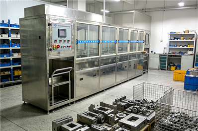
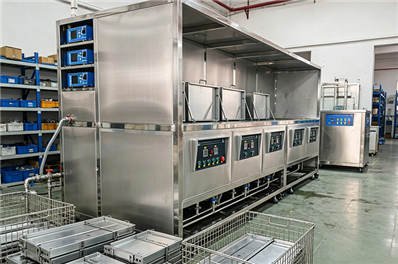
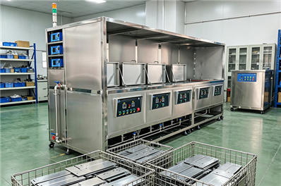
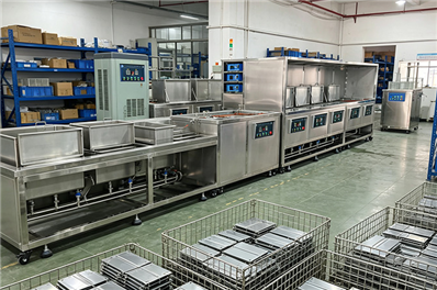
Whale Cleen has established itself as a trusted manufacturer of ultrasonic cleaning equipment with applications across industrial manufacturing sectors. With a 10,000-square-meter production base and a history of delivering professional cleaning solutions since 2003, Whale Cleen combines technical expertise with manufacturing capacity [0†L2-L5].
Customizable Configurations for Wafer Cleaning
Unlike manufacturers offering only standard off-the-shelf systems, Whale Cleen can customize ultrasonic cleaning equipment to match specific wafer cleaning requirements. This customization capability extends to frequency selection (from conventional ultrasonic to megasonic ranges), tank sizing to accommodate standard wafer cassettes, and automation levels from manual-load to fully PLC-controlled systems.
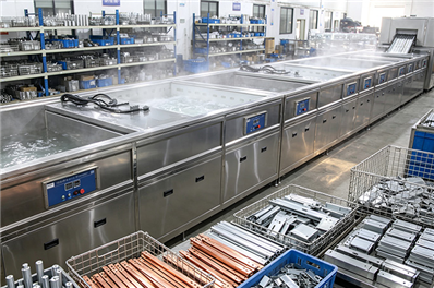
Multi-Stage Cleaning Lines for Superior Results
For silicon wafer cleaning, a single cleaning stage is rarely sufficient. Whale Cleen designs multi-stage cleaning lines that separate cleaning, rinsing, and drying functions into distinct process tanks [4†L40-L44]. This design serves two critical purposes: it prevents cross-contamination between cleaning baths, and it allows each stage to optimize its chemistry and process parameters independently. The result is more thorough contamination removal and longer chemical bath life.
Uniform Cavitation for Consistent Batch Cleaning
A common challenge in ultrasonic cleaning is acoustic shadowing—areas within the cleaning tank where cavitation intensity is reduced, leading to uneven cleaning. Whale Cleen’s engineering addresses this through optimized transducer array designs that deliver uniform cavitation across the entire cleaning zone. For wafer cleaning, uniform cavitation means every wafer in a batch receives the same cleaning intensity, eliminating the risk of under-cleaned or over-cleaned units.
Industrial-Grade Reliability
Semiconductor manufacturing demands equipment that runs continuously with minimal downtime. Whale Cleen ultrasonic cleaning machines are built for industrial applications, with robust construction, sealed electronic components, and designs rated for 24/7 operation. This reliability translates to predictable production schedules and lower total cost of ownership compared to consumer-grade or light-industrial equipment.
Eco-Friendly Operation
Environmental compliance is increasingly critical in semiconductor manufacturing. Whale Cleen systems support reduced chemical consumption and water usage compared to traditional cleaning methods, helping facilities meet environmental targets while controlling operating costs. Multi-stage designs extend chemical bath life, reducing both consumable purchases and waste disposal requirements [4†L40-L44].
When semiconductor manufacturers evaluate ultrasonic cleaning equipment suppliers, they typically consider four criteria: cleaning effectiveness, process consistency, equipment reliability, and total cost of ownership. Whale Cleen addresses each of these requirements:
Cleaning effectiveness: Multi-stage designs with customizable frequencies ensure contaminants are thoroughly removed from every wafer surface.
Process consistency: Uniform cavitation distribution produces identical results batch after batch, eliminating process variability.
Equipment reliability: Industrial construction and quality components deliver dependable 24/7 operation.
Total cost of ownership: Reduced chemical consumption, extended bath life, and lower rework rates generate ongoing operational savings.
Silicon wafer cleaning presents unique challenges: microscopic particles hidden in nanometer-scale features, delicate surfaces vulnerable to mechanical damage, and the absolute requirement for consistent, repeatable results. Ultrasonic cleaning technology addresses these challenges through the physical principle of cavitation—using sound waves to generate cleaning action that reaches every surface, contacts nothing, and produces uniform results batch after batch.
Whale Cleen ultrasonic cleaning machines deliver these advantages with industrial-grade reliability, customizable configurations for wafer-specific requirements, and multi-stage designs that maximize cleaning effectiveness while minimizing chemical consumption. For semiconductor manufacturers seeking to improve wafer cleanliness, protect fragile device features, and lower cleaning costs, ultrasonic cleaning—and the Whale Cleen equipment that implements it—represents the preferred choice.