I. Challenges in Cleaning Electronic Semiconductor Devices
With the constant miniaturization and increased integration of electronic devices, semiconductor components face challenges related to the presence of minute particles, residues, and oxide layers. These issues can adversely impact the performance and reliability of semiconductor devices. Conventional cleaning methods, such as spray cleaning, immersion, and aerosol cleaning, often fall short in meeting the stringent cleaning requirements for microscopic devices. Moreover, these methods may introduce static charges, water spots, and other contaminants, affecting cleanliness and stability.
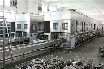
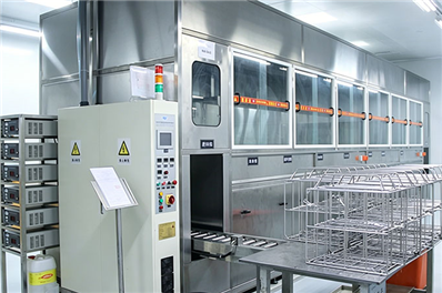
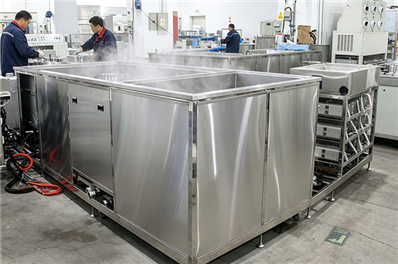
II. Advantages of Ultrasonic Cleaning Technology
Comprehensive Coverage of Microstructures: Ultrasonic cleaning technology utilizes high-frequency vibrations to generate microscopic bubbles in the cleaning solution, creating implosive effects and microstreaming. This capability ensures thorough coverage of the surfaces and microgaps of electronic semiconductor devices, effectively removing adhered contaminants.
Non-contact Cleaning: Ultrasonic cleaning is a non-contact method, ensuring that devices undergo the cleaning process without mechanical collisions. This feature is particularly advantageous for maintaining the integrity of device surfaces, making it suitable for applications where surface damage is a concern.
Residue-Free Cleaning: The intense liquid flow generated by ultrasonic cleaning thoroughly flushes the surfaces of semiconductor devices. This eliminates concerns about residual contaminants that may persist with traditional cleaning methods, ensuring a high level of cleanliness.
High Controllability: Ultrasonic cleaning equipment is equipped with adjustable frequency and power settings. This flexibility allows customization based on the specific characteristics of electronic semiconductor devices, enhancing the controllability and adaptability of the cleaning process.
III. Applications of Ultrasonic Cleaning Technology in Electronic Semiconductor Devices
Integrated Circuits (ICs) Cleaning: IC chips often possess intricate microstructures crucial for their performance. Ultrasonic cleaning technology can precisely clean IC chips, ensuring that their surfaces are free from microscopic impurities, thus enhancing device efficiency and reliability.
Printed Circuit Board (PCB) Cleaning: PCBs, as foundational components of electronic devices, often contain numerous electronic elements and tiny conductive traces. Ultrasonic cleaning efficiently removes contaminants from these fine structures, ensuring proper connectivity between electronic components.
Pre-assembly Cleaning of Semiconductor Devices: Cleaning before the assembly of semiconductor devices is a critical step. Ultrasonic cleaning ensures a thorough and efficient cleaning process, reducing the likelihood of post-assembly defects.
Cleaning of Laser Diodes: Laser diodes, integral to optoelectronic devices, demand high precision in cleaning to maintain optimal performance. Ultrasonic cleaning technology guarantees a pure surface for laser diodes, contributing to their enhanced functionality.
IV. Future Trends and Prospects
Intelligent Cleaning Equipment: The future of ultrasonic cleaning equipment is expected to incorporate advanced sensing technologies and automated control systems. This development aims to achieve real-time monitoring and adjustment of cleaning parameters, enhancing efficiency and consistency.
Environmentally Friendly Cleaning Agents: With increasing environmental awareness, future ultrasonic cleaning solutions may focus on the development of environmentally friendly cleaning agents. This aligns with the industry's demand for sustainable practices in semiconductor device manufacturing.
Multifunctional Ultrasonic Cleaning Equipment: Future ultrasonic cleaning equipment is anticipated to be more multifunctional, catering to diverse types, sizes, and characteristics of electronic semiconductor devices. This adaptability will further broaden the scope of ultrasonic cleaning applications.
International Standardization: As the semiconductor industry becomes more globalized, ultrasonic cleaning technology may play a role in shaping and influencing international standards for semiconductor device cleaning. This ensures consistency and comparability in cleaning processes across the industry.
V. Conclusion
Ultrasonic cleaning technology stands as a transformative solution to the challenges associated with cleaning electronic semiconductor devices. Its efficiency, non-destructive cleaning methodology, and potential for future innovation position it as a valuable tool in the realm of electronic technology. Looking ahead, as technology continues to evolve, ultrasonic cleaning is poised to make further strides in addressing the intricate cleaning demands of electronic semiconductor devices, contributing to the reliability and performance of semiconductor technologies.